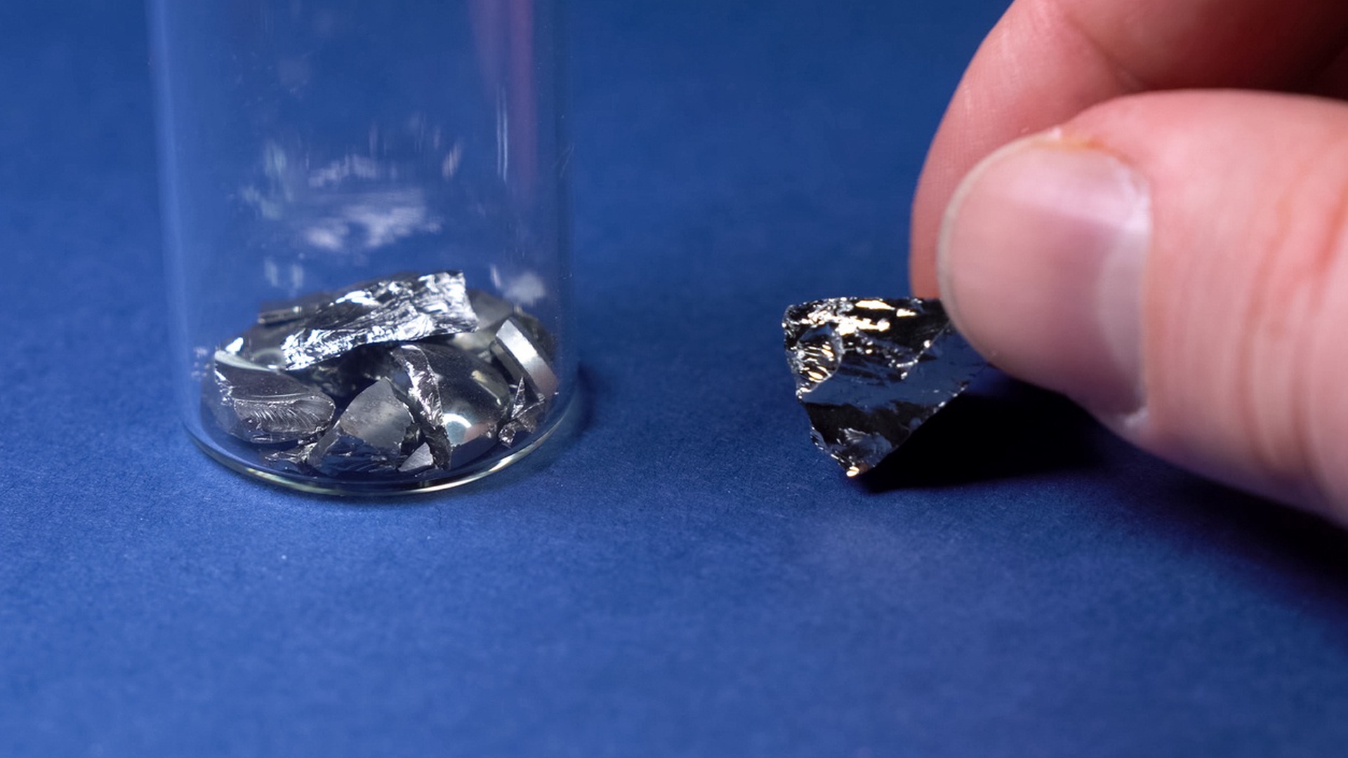
Germanium (Ge) was the material used in the first transistor, which was invented by Bardeen, Brattain, and Shockley at Bell Laboratories in 1947. This marked a significant milestone in the semiconductor industry. However, due to its practical superiorities and intrinsic properties, silicon (Si) soon became the preferred material over Ge. As a result, Si became the primary material in the industry, driving the miniaturization and large-scale integration of modern electronic devices. While Ge was initially used in limited fields such as g-ray detectors and infrared optics, it experienced a period of disinterest. However, since the 1990s, Ge has once again garnered keen interest for its applications in ultrafast electronic devices and its favorable intrinsic carrier mobility. As a result, numerous research groups around the world, particularly in Belgium, have renewed their efforts to develop Ge as a material for mainstream semiconductors. This resurgence has led to the promotion of large-crystal growth and the fabrication of electronic devices by Belgian research groups and companies.
Germanium crystal growth techniques have improved to address production challenges. Single crystal growth starts with a dislocation-free Ge seed crystal, which is dipped into the Ge melt to initiate growth. Sometimes, silicon (Si) seeds are used, resulting in a dilute SiGe alloy. To reduce dislocation generation, the Dash necking technique is employed, which involves reducing the crystal diameter to about 2-4 mm, allowing dislocations from the seed to escape through the thin neck, resulting in a dislocation-free crystal. The Low Temperature Gradient (LTG) CZ method has been developed to grow large Ge crystals with minimal dislocation densities, using a temperature gradient of less than 1 K/cm. Additionally, oxygen doping has proven effective in growing oxygen-enriched Ge crystals with extremely low dislocation densities by using oxygen atoms from GeO₂ powder in a B₂O₃-covered melt to suppress dislocation generation.
Germanium's physical properties, particularly its mechanical strength and dislocation behavior, pose distinct challenges. Ge exhibits lower mechanical strength than silicon, with its yield strength increasing as temperature decreases until a ductile-to-brittle transition is reached. The stress-intensity factor (K_IC) for Ge is 0.6 MPa m¹/², slightly lower than Si's 0.7 MPa m¹/². Dislocations in Ge move more rapidly than in Si, and their velocity is influenced by temperature, stress, and impurities. For example, impurities such as gallium (Ga) and oxygen (O) can suppress dislocation nucleation, while arsenic (As) does not have the same effect. This ability to control dislocation behavior through impurity doping is crucial for optimizing material performance in various applications. Additionally, Ge's lower thermal conductivity than Si contributes to greater thermoelastic stress during crystal growth, complicating the production of large, dislocation-free Ge crystals.
Property |
Germanium (Ge) |
Silicon (Si) |
Atomic Weight (M) |
72.64 |
28.09 |
Atomic Radius (r, nm) |
0.123 |
0.117 |
Lattice Constant (a, nm) |
0.56575 |
0.5431 |
Density (ρ, g/cm³) |
5.33 |
2.33 |
Atomic Number in a Unit Volume (N, cm⁻³) |
4.42 × 10²² |
5 × 10²² |
Bandgap (@0K/@RT, eV) |
0.74/0.66 |
1.17/1.12 |
Intrinsic Carrier Density (@RT, cm⁻³) |
2.5 × 10¹³ |
1.45 × 10¹³ |
Effective Mass |
||
- Electron Density of State (mₑᵈ/m₀) |
0.19 |
0.16 |
- Longitudinal (mₗₑ/m₀) |
1.64 |
0.98 |
- Transversal (mₜₑ/m₀) |
0.082 |
0.19 |
- Hole Density of State (mₕᵈ/m₀) |
0.34 |
0.81 |
- Light (mₗₕ/m₀) |
0.044 |
0.16 |
- Heavy (mₕₕ/m₀) |
0.28 |
0.49 |
Mobility |
||
- Electron (mₑ, cm²/Vs) |
3900 |
1500 |
- Hole (mₕ, cm²/Vs) |
1900 |
450 |
Dielectric Constant (ε) |
16.0 |
11.9 |
Refractivity (n) |
4.01 |
3.42 |
Elastic Constant (@RT) |
||
- C₁₁ (GPa) |
129 |
166 |
- C₁₂ (GPa) |
48.3 |
64.0 |
- C₄₄ (GPa) |
67.1 |
79.6 |
Shear Modulus (G, GPa) |
48.9 |
60.5 |
Strength (@TM/@(2/3)TM, GPa) |
0.3/25 |
1.0/40 |
Surface Energy (111, γ, erg/cm²) |
1060 |
1230 |
Linear Thermal Expansion (@RT/@TM, K⁻¹) |
5.9 × 10⁻⁶ / 2.6 × 10⁻⁶ |
9 × 10⁻⁶ / 4.4 × 10⁻⁶ |
Thermal Conductivity (@RT/@TM, W/m·K) |
58/24 |
157/31 |
Gibbs Standard Free Energy of Dioxide Formation (@TM, ΔG, kJ/mol) |
3.41 |
6.80 |
Germanium crystals have seen significant advances in growth techniques, mechanical properties, and applications. While they are now comparable to silicon in many respects, they still face challenges, including lower mechanical strength and difficulty producing large, dislocation-free crystals. However, with ongoing research and development, including techniques such as oxygen doping and advanced alloy systems, Ge remains a valuable material in various high-tech applications, from infrared optics to advanced electronics and radiation detection. The unique properties of Ge, combined with innovative engineering, hold promise for future advancements in semiconductor technology.